Abstract
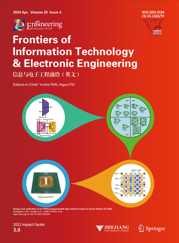
This paper proposes a kind of based on technology. By programming , all three-bit (LUT3) functions, partial four-bit (LUT4) functions, latch functions, and d flip flop (DFF) with enable and reset functions can be realized. Because PLE uses a choice of operational logic (COOL) approach for the operation of logic functions, it allows any logic circuit to be implemented at any ratio of combinatorial logic to register. This intrinsic property makes it close to the basic application specific integrated circuit (ASIC) cell in terms of fine granularity, thus allowing ASIC-like cell-based mappers to apply all their optimization potential. By measuring and PLE circuits, the results show that the “on” state driving current of the is about 245.52 μA, and that the “off” state leakage current is about 0.1 pA. The programmable function of PLE works normally. The delay of the typical combinatorial logic operation AND3 is 0.69 ns, and the delay of the sequential logic operation DFF is 0.65 ns, both of which meet the requirements of the design technical index.


 京公网安备 11010502051620号